Digital Design
Schematics Due Wed April 3rd by 11:59pm in your Lab06 GitHub repo
Links
Tests: https://github.com/USF-CS631-S24/tests
Autograder: https://github.com/phpeterson-usf/autograder
Requirements
You will learn the basics of digital logic and digital circuits with the goal of learning enough to build a working computer processor. We will use the Digital application to build and simulate digital circuits:
https://github.com/hneemann/Digital
For this lab your are going to build and simulate some simple circuits.
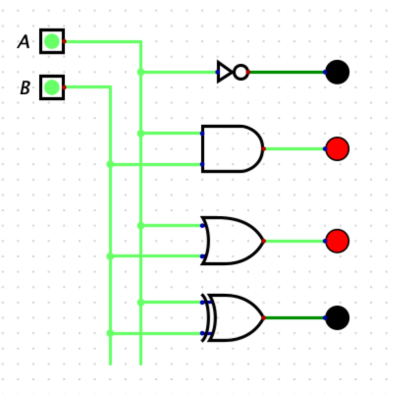
Circuit 1: LEDs
- You will build a circuit in with two inputs and 4 LED output that shows how 4 basics gates work: NOT, AND, OR, and XOR.
- The LED will turn red when the input is high (1) and black when in the input is low (0).
- Here is a screen shot of the circuit you need to build and simulate. Note that you need to add labels to the inputs (A and B):
Circuit 2: Max2
Consider the C code fragment below:
if (a > b) {
    r = a;
} else {
    r = b;
}
- We will assume that a, b, and r are 2-bit values. That is, the only values a, b, and r can be are 0 (0b00), 1 (0b01), 2 (0b10), or 3 (0b11).
- Your job is to use sum-of-products to come up with a Boolean algebra equation and a circuit that will compute the max value r (which is also a 2-bit value).
- Your inputs will be
a1,a0,b1,b0and your outputs will ber1andr0. So, you will have two Boolean equations, one forr1and one forr0. - Since there are 4 inputs you will have 2^4 (16) rows in your truth table.
- Submit a working circuit that correctly produces the max value of the two inputs. You do not need to submit the truth table or Boolean algebra equation.
- Your circuit must have input names
a1,a0,b1, andb0. - Hint: you can build your sum-of-products by only considering the rows with output of 0, then invert the resulting equation. This will minimize the number of product terms.
- Your file must be called
max2.dig
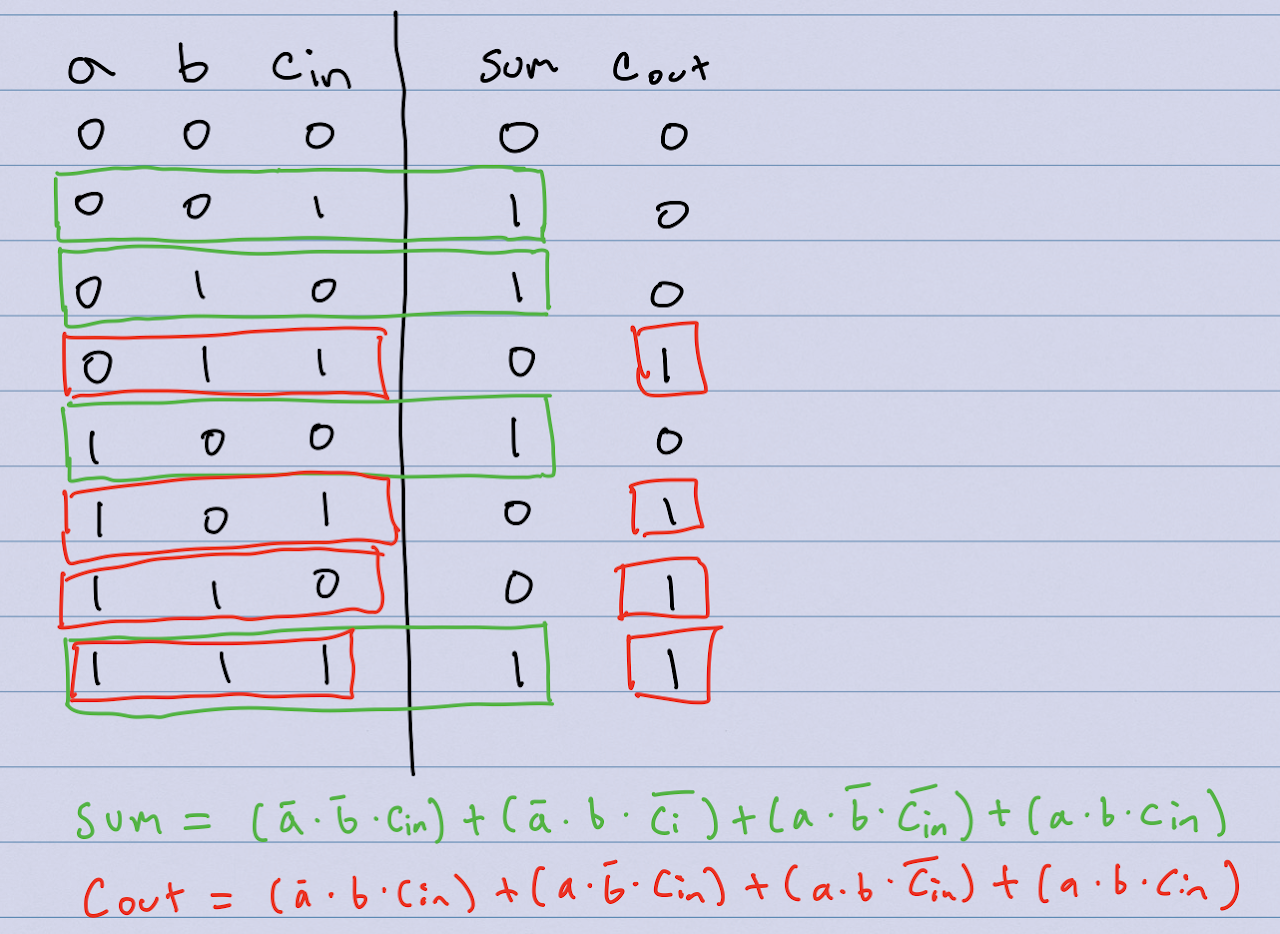
Circuit 3: 1-bit full adder
- In lecture, we built a 1-bit half adder (that is, an adder which does not have a carry-in) and showed the Boolean Algebra equation for a 1-bit full adder.
- You will build a 1-bit full adder in Digital, including a carry-in (
cin) and a carry-out (cout). Your circuit must have inputs nameda,b, andcin, and outputs namedsumandcout. - Your file must be named
1-bit-full-adder.dig - Here are the truth table and sum-of-products equations for
sumandcout
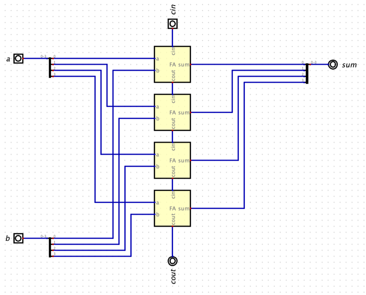
Circuit 4: 8-bit Ripple Carry Adder
- Using your 1-bit full adder, build an 8-bit Ripple Carry Adder.
- Configure the 1-bit full adder symbol so that the cin is on the top and the cout in on the bottom. You will have to increase the height and width of the 1-bit full adder symbol in Edit -> Circuit Specific Settings.
- Your 8-bit Adder should have two 8-bit inputs (a and b), a 1-bit carry-in (cin), an 8-bit sum output, and a 1-bit carry-out (cout) output.
- You can configure inputs and outputs to be multiple bit inputs.
- You can use a splitter (in the wires section) to split an n-bit wire (a bus) into multiple 1-bit wires (actually the splitter is very flexible and can do more than this). You can also use a splitter to combine multiple 1-bit wires to create a n-bit wire (bus).
- Your file must be called
8-bit-ripple-carry-adder.dig - Here is a picture of what a 4-bit Ripple Carry Adder looks like. Yours does not need to be identical.
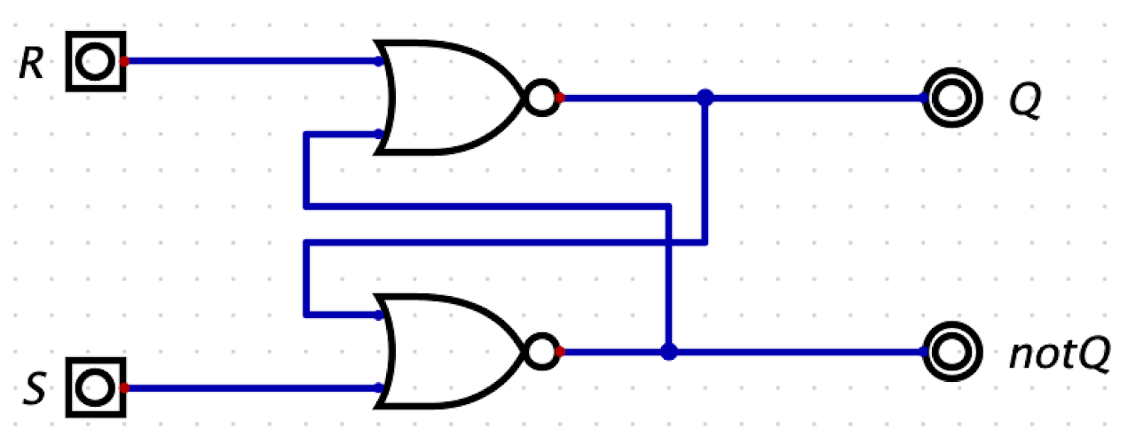
Circuit 5: SR Latch
A set-reset latch uses “cross coupling” to allow the two NOR gates to store 1-bit of information. Here are valid SR Latch states:
S R | Q notQ
0 0 | 0    1
1 0 | 1    0
0 0 | 1    0
0 1 | 0    1
0 0 | 0    1
1 1 | X    X (UNDEFINED)
Note the SR Latch does not have the clock as an input.
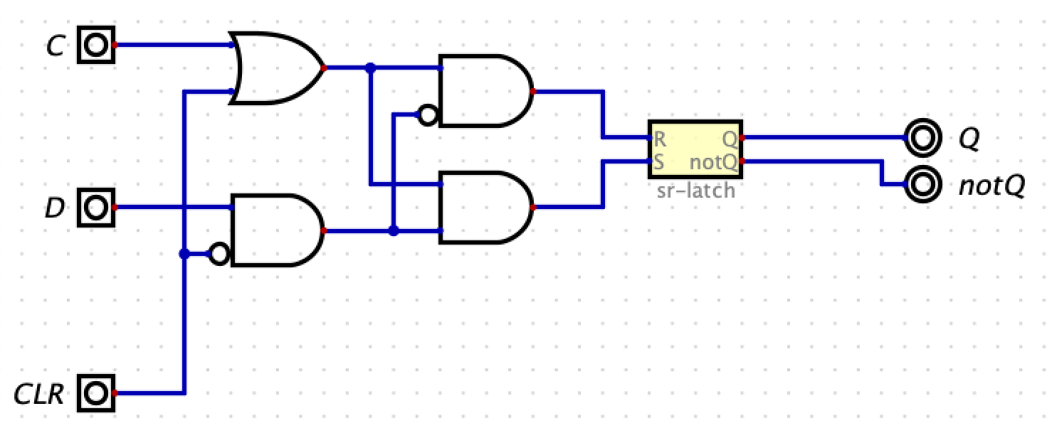
Circuit 6: D Latch with Clear
The D Latch is built using the SR Latch. The clock is used to latch the D value. When the clock is high, the value D is stored in the SR Latch. When the clock is low, the D Latch holds its previously stored value. The CLR (clear) line sets the SR Latch to 0.
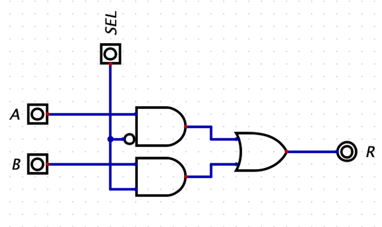
Circuit 7: 1-bit 2-input Multiplexor (MUX)
The multiplexor is an extremely useful circuit that is used to select between multiple inputs. We need a MUX to build the D Flipflop with Enable and Clear.
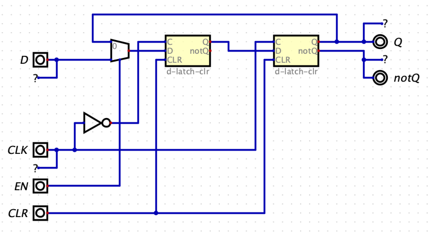
8: D Flip-flop with Enable and Clear
Unlike the D Latch, the D Flip-flop only stores the input value D on the rising edge of the clock (edge triggered). Using an edge triggered latch allows us to know when the state element will be updated.
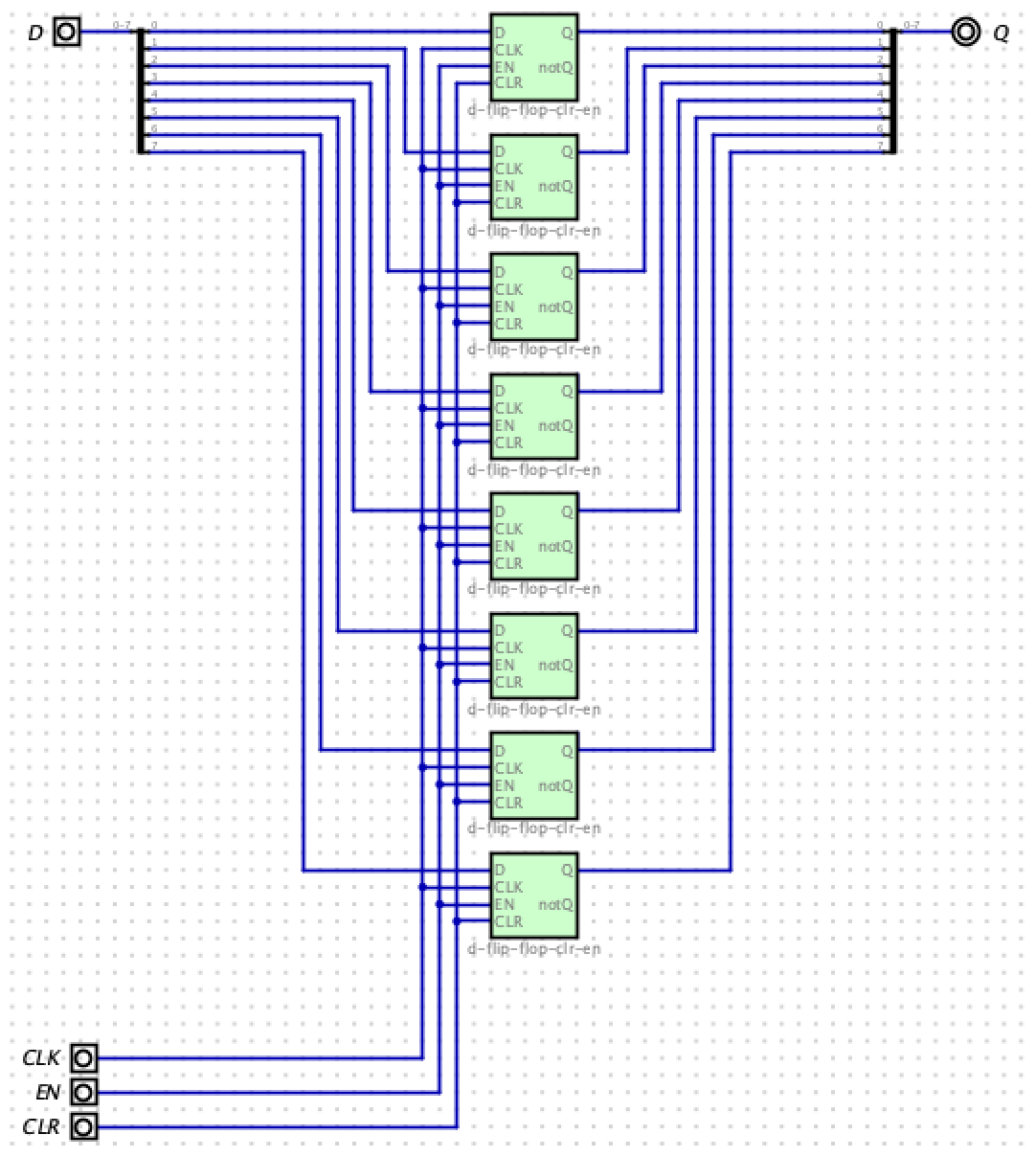
9: 8-bit Register with Enable and Clear
We can build an N-bit register using N D Flip-flops.
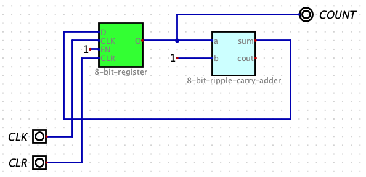
Circuit 10: 8-bit Counter
We can now build and 8-bit counter using an 8-bit adder and an 8-bit register. Name your file 8-bit-counter.dig.
Grading Rubric
Automated testing
100 pts: Automated tests
Circuit Quality
Keep your circuits organized and symmetric. Do not use diagonal wires even though Digital allows you to do so. For the circuit labs we will not look at circuit quality, but for the projects we will. However, it is best just to build clean circuits from the beginning. You also need to have a clean repo with no extra files.